- 您现在的位置:买卖IC网 > Sheet目录312 > AT27BV4096-12VI (Atmel)IC OTP 4MBIT 120NS 40VSOP
AT27BV4096
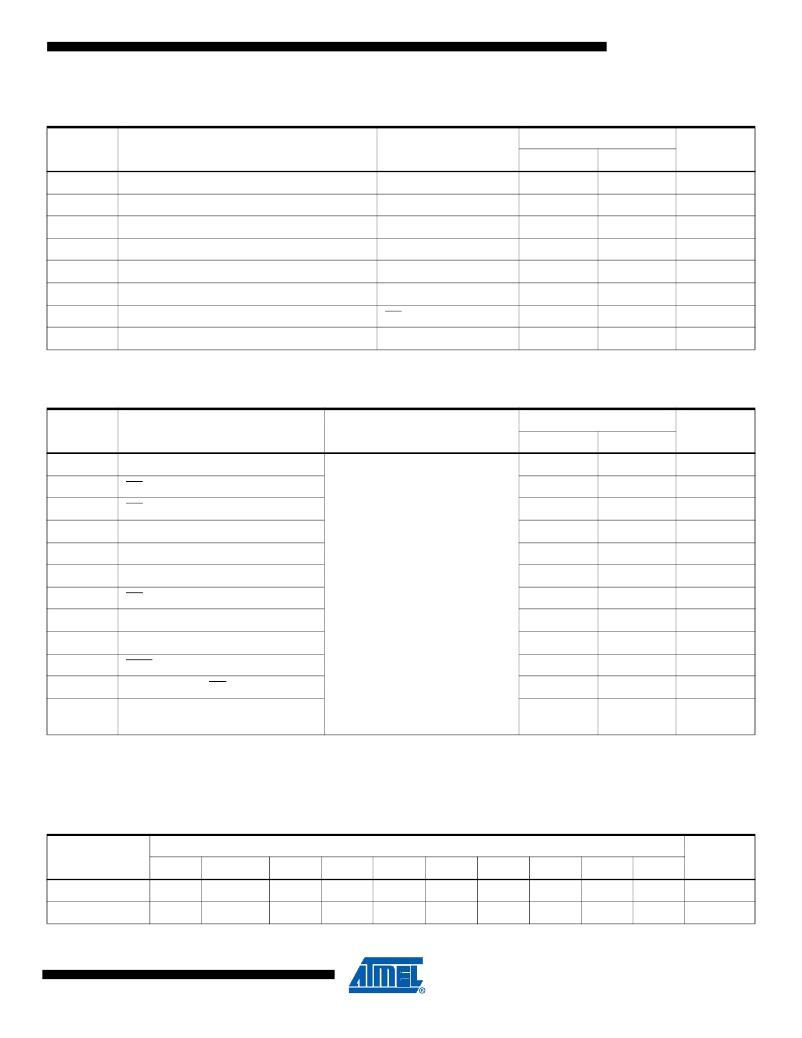
15. DC Programming Characteristics
T A = 25 ± 5 ° C, V CC = 6.5 ± 0.25V, V PP = 13.0 ± 0.25V
Limits
Symbol
Parameter
Test Conditions
Min
Max
Units
I LI
V IL
V IH
V OL
Input Load Current
Input Low Level
Input High Level
Output Low Voltage
V IN = V IL , V IH
I OL = 2.1 mA
-0.6
2.0
± 10
0.8
V CC + 0.1
0.4
m A
V
V
V
V OH
I CC2
Output High Voltage
V CC Supply Current (Program and Verify)
I OH = -400 μA
2.4
50
V
mA
I PP2
V ID
V PP Supply Current
A9 Product Identification Voltage
CE = V IL
11.5
30
12.5
mA
V
16. AC Programming Characteristics
T A = 25 ± 5 ° C, V CC = 6.5 ± 0.25V, V PP = 13.0 ± 0.25V
Limits
PGM Program Pulse Width
Symbol
t AS
t CES
t OES
t DS
t AH
t DH
t DFP
t VPS
t VCS
t PW
t OE
t PRT
Parameter
Address Setup Time
CE Setup Time
OE Setup Time
Data Setup Time
Address Hold Time
Data Hold Time
OE High to Output Float Delay (2)
V PP Setup Time
V CC Setup Time
(3)
Data Valid from OE
V PP Pulse Rise Time During
Programming
Test Conditions (1)
Input Rise and Fall Times:
(10% to 90%) 20 ns
Input Pulse Levels:
0.45V to 2.4V
Input Timing Reference Level:
0.8V to 2.0V
Output Timing Reference Level:
0.8V to 2.0V
Min
2
2
2
2
0
2
0
2
2
47.5
50
Max
130
52.5
150
Units
μs
μs
μs
μs
μs
μs
ns
μs
μs
μs
ns
ns
Notes:
1. V CC must be applied simultaneously or before V PP and removed simultaneously or after V PP .
2. This parameter is only sampled and is not 100% tested. Output Float is defined as the point where data is no longer driven –
see timing diagram.
3. Program Pulse width tolerance is 50 μsec ± 5%.
17. Atmel’s AT27BV4096 Integrated Product Identification Code (1)
Pins
Hex
Codes
Manufacturer
Device Type
A0
0
1
O15-O8
0
0
O7
0
1
O6
0
1
O5
0
1
O4
1
1
O3
1
0
O2
1
1
O1
1
0
O0
0
0
Data
001E
00F4
Note:
1. The AT27BV4096 has the same Product Identification Code as the AT27C4096. Both are programming compatible.
9
0640E–EPROM–8/07
发布紧急采购,3分钟左右您将得到回复。
相关PDF资料
AT27BV512-70JU
IC OTP 512KBIT 70NS 32PLCC
AT27C010-45JU
IC OTP 1MBIT 45NS 32PLCC
AT27C020-55PU
IC OTP 2MBIT 55NS 32DIP
AT27C040-90PU
IC OTP 4MBIT 90NS 32DIP
AT27C080-90PU
IC OTP 8MBIT 90NS 32DIP
AT27C1024-45PU
IC OTP 1MBIT 45NS 40DIP
AT27C2048-55JU
IC OTP 2MBIT 55NS 44PLCC
AT27C256R-45PU
IC OTP 256KBIT 45NS 28DIP
相关代理商/技术参数
AT27BV409615JC
制造商:Atmel Corporation 功能描述:
AT27BV4096-15JC
功能描述:可擦除可编程ROM 4M bit RoHS:否 制造商:Maxim Integrated 类型: 存储容量:1024 bit 组织:1 K x 1 接口类型: 工作电流:5 uA 编程电压: 工作电源电压:2.8 V to 6 V 最大工作温度:+ 85 C 安装风格:Through Hole 封装 / 箱体:TO-92
AT27BV4096-15JI
功能描述:IC OTP 4MBIT 150NS 44PLCC RoHS:否 类别:集成电路 (IC) >> 存储器 系列:- 标准包装:32 系列:- 格式 - 存储器:闪存 存储器类型:FLASH 存储容量:1M (128K x 8) 速度:120ns 接口:并联 电源电压:2.7 V ~ 3.6 V 工作温度:0°C ~ 70°C 封装/外壳:32-LCC(J 形引线) 供应商设备封装:32-PLCC 包装:管件 其它名称:AT49BV00112JC
AT27BV4096-15VC
功能描述:可擦除可编程ROM 4M bit RoHS:否 制造商:Maxim Integrated 类型: 存储容量:1024 bit 组织:1 K x 1 接口类型: 工作电流:5 uA 编程电压: 工作电源电压:2.8 V to 6 V 最大工作温度:+ 85 C 安装风格:Through Hole 封装 / 箱体:TO-92
AT27BV4096-15VI
功能描述:IC OTP 4MBIT 150NS 40VSOP RoHS:否 类别:集成电路 (IC) >> 存储器 系列:- 标准包装:32 系列:- 格式 - 存储器:闪存 存储器类型:FLASH 存储容量:1M (128K x 8) 速度:120ns 接口:并联 电源电压:2.7 V ~ 3.6 V 工作温度:0°C ~ 70°C 封装/外壳:32-LCC(J 形引线) 供应商设备封装:32-PLCC 包装:管件 其它名称:AT49BV00112JC
AT27BV512
制造商:ATMEL 制造商全称:ATMEL Corporation 功能描述:512K (64K x 8) Unregulated Battery-Voltage High-Speed OTP EPROM
AT27BV512_07
制造商:ATMEL 制造商全称:ATMEL Corporation 功能描述:512K (64K x 8) Unregulated Battery-Voltage High-Speed OTP EPROM
AT27BV512-12JC
功能描述:IC OTP 512KBIT 120NS 32PLCC RoHS:否 类别:集成电路 (IC) >> 存储器 系列:- 标准包装:96 系列:- 格式 - 存储器:闪存 存储器类型:FLASH 存储容量:1M (64K x 16) 速度:150ns 接口:并联 电源电压:3 V ~ 3.6 V 工作温度:0°C ~ 70°C 封装/外壳:48-TFSOP(0.724",18.40mm 宽) 供应商设备封装:48-TSOP 包装:托盘
